Switching light with a silver atom
Researchers working under Juerg Leuthold, Professor of Photonics and Communications, have created the world’s smallest integrated optical switch. Applying a small voltage causes an atom to relocate, turning the switch on or off.
The quantity of data exchanged via communications networks around the globe is growing at a breathtaking rate. The volume of data for wired and mobile communications is currently increasing by 23% and 57% respectively every year. It is impossible to predict when this growth will end. This also means that all network components must constantly be made more efficient.
These components include so-called modulators, which convert the information that is originally available in electrical form into optical signals. Modulators are therefore nothing more than fast electrical switches that turn a laser signal on or off at the frequency of the incoming electrical signals. Modulators are installed in data centres in their thousands. However, they all have the disadvantage of being quite large. Measuring a few centimetres across, they take up a great deal of space when used in large numbers.
From micromodulators to nanomodulators
Six months ago, a working group led by Jürg Leuthold, Professor of Photonics and Communications already succeeded in proving that the technology could be made smaller and more energy-efficient. As part of that work, the researchers presented a micromodulator measuring just 10 micrometres across – or 10,000 times smaller than modulators in commercial use (see ETH News).
Leuthold and his colleagues have now taken this to the next level by developing the world’s smallest optical modulator. And this is probably as small as it can get: the component operates at the level of individual atoms. The footprint has therefore been further reduced by a factor of 1,000 if you include the switch together with the light guides. However, the switch itself is even smaller, with a size measured on the atomic scale. The team’s latest development was recently presented in the journal Nano Letters.
In fact, the modulator is significantly smaller than the wavelength of light used in the system. In telecommunications, optical signals are transmitted using laser light with a wavelength of 1.55 micrometres. Normally, an optical device can not be smaller than the wavelength it should process. “Until recently, even I thought it was impossible for us to undercut this limit,” stresses Leuthold.
New structure
But his senior scientist Alexandros Emboras proved the laws of optics wrong by successfully reconfiguring the construction of a modulator. This construction made it possible to penetrate the order of magnitude of individual atoms, even though the researchers were using light with a “standard wavelength”.

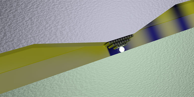
Emboras’s modulator consists of two tiny pads, one made of silver and the other of platinum, on top of an optical waveguide made of silicon. The two pads are arranged alongside each other at a distance of just a few nanometres, with a small bulge on the silver pad protruding into the gap and almost touching the platinum pad.
Short circuit thanks to a silver atom
And here’s how the modulator works: light entering from an optical fibre is guided to the entrance of the gap by the optical waveguide. Above the metallic surface, the light turns into a surface plasmon. A plasmon occurs when light transfers energy to electrons in the outermost atomic layer of the metal surface, causing the electrons to oscillate at the frequency of the incident light. These electron oscillations have a far smaller diameter than the ray of light itself. This allows them to enter the gap and pass through the bottleneck. On the other side of the gap, the electron oscillations can be converted back into optical signals.
If a voltage is now applied to the silver pad, a single silver atom or, at most, a few silver atoms move towards the tip of the point and position themselves at the end of it. This creates a short circuit between the silver and platinum pads, so that electrical current flows between them. This closes the loophole for the plasmon; the switch flips and the state changes from “on” to “off” or vice versa. As soon as the voltage falls below a certain threshold again, a silver atom moves back. The gap opens, the plasmon flows, and the switch is “on” again. This process can be repeated millions of times.
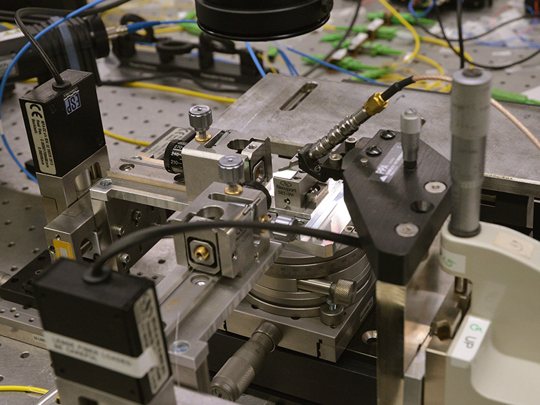
ETH Professor Mathieu Luisier, who participated in this study, simulated the system using a high-performance computer at the CSCS in Lugano. This allowed him to confirm that the short circuit at the tip of the silver point is brought about by a single atom.
A truly digital signal
As the plasmon has no other options than to pass through the bottleneck either completely or not at all, this produces a truly digital signal – a one or a zero. “This allows us to create a digital switch, as with a transistor. We have been looking for a solution like this for a long time,” summarises Leuthold.
As yet, the modulator is not ready for series production. Although it has the advantage of operating at room temperature, unlike other devices that work using quantum effects at this order of magnitude, it still remains very slow for a modulator: so far, it only works for switching frequencies in the megahertz range or below. The ETH researchers want to fine-tune it for frequencies in the gigahertz to terahertz range.
Improving the lithography process
The researchers also want to further improve the lithography method, which was redeveloped by Emboras from scratch to build the parts, so that components like this can be produced reliably in future. At present, fabrication is only successful in one out of every six attempts. Nevertheless, the researchers consider this a success, as lithography processes on the atomic scale remain uncharted territory.
In order to continue his research into the nanomodulator, Leuthold has strengthened his team. However, he points out that greater resources would be required to develop a commercially available solution. Despite this, the ETH professor is confident that he and his team will be able to present a practicable solution within the next few years.
References
A. Emboras, J. Niegemann, P. Ma, C. Haffner, A. Pedersen, M. Luisier, C. Hafner, T. Schimmel, and J. Leuthold, Atomic Scale Plasmonic Switch, Nano Letters 16, 709-714 (2016). DOI: external page10.1021/acs.nanolett.5b04537