Symposium in the honour of Heinrich Rohrer
At ETH Zurich, on October 31, leading scientists paid tribute to the achievements of Heinrich Rohrer. The Nobel Prize Laureate in Physics and ETH alumnus passed away earlier this year.
“Heinrich Rohrer was an inspiring figure in science and played a decisive role in the development of modern nanotechnology,” says Christian Degen from the Laboratory for Solid State Physics. Degen, together with Gianni Blatter, a theoretical physicist at ETH, and colleagues Walter Riess and Gerd Binnig from the IBM research laboratory in Rüschlikon, organised a symposium in the honour of Heinrich Rohrer. Rohrer studied at ETH in the 1950s and joined the IBM research laboratory in 1963. In 1986, Binnig and Rohrer received the Nobel Prize for the invention of the scanning tunnelling microscope.
“Even though it was obvious that this was a significant instrument, nobody could have imagined how widely it would be used today,” Blatter explains. The scanning tunnelling microscope – also known as the STM – uses the sensitive tunnelling current between a sharp tip and the surface under study. The STM not only renders individual atoms visible, but also allows the manipulation and positioning of specific atoms. Nowadays, the STM and other related instruments are indispensable tools used in the fields of physics, electronics, chemistry, biology, and material science. The symposium united early colleagues of Rohrer, several STM pioneers, as well as leading scientists in whose research the scanning microscope plays a central role.
Specific positioning of atoms
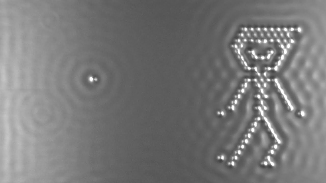
One of these scientists is Andreas Heinrich, a researcher at the IBM Almaden Research Center in San Jose. The laboratory is famous for spelling out the tiniest IBM logo by moving 35 Xenon atoms into place using a scanning tunnelling microscope. Today, Heinrich’s goal is to build the components of a computer out of single atoms. In addition, he has also ‘shot’ the world’s smallest film: “A Boy and his Atom”, which has been downloaded several million times from Youtube.
The role of the Swiss watch industry
The Swiss watch industry also found its way into this field of research: the atomic force microscope (AFM), which was developed a few years later, can show atoms on insulating surfaces. To achieve this, the imaging tip is mounted on a flexible lever arm that is brought into oscillation. The changes in amplitude and frequency then provide information about the atomic force profile of the surface under investigation. As Franz Giessibl from the University of Regensburg explained, quartz tuning forks of electronic watches make excellent lever arms for the AFM. The AFM provides new opportunities for chemistry and biology because it can operate in air or liquids – for example, functional organic nanosystems can be investigated and improved, as was highlighted at the symposium.
Whenever one looks at carbon nanotubes, the properties of graphene or new magnetic storage devices in nanotechnology, the insights and progress the research community gained through the work of Binnig and Rohrer is evident. “Without the scanning tunnelling microscope, modern nanotechnology is simply inconceivable,” says Blatter. To pay appropriate tribute to the achievements of Rohrer and Binnig, the joint research centre of IBM and ETH Zürich was named the Binnig and Rohrer Nanotechnology Center on its inauguration in 2011.